A (Solder) Bridge To Nowhere: What Is a Solder Bridge and How to Avoid Them in PCB Design
What is a solder bridge?
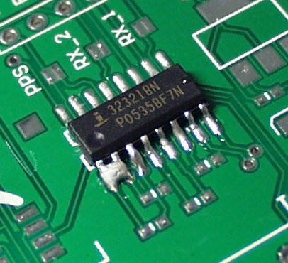
A solder bridge forms when two points on a circuit board that are not designed to be electrically connected are inadvertently connected by solder over the top of the PCB solder mask. This creates an electrical short that can wreak all kinds of havoc, depending on what the two points that are shorted together are designed to do.

An example of a solder bridge
What causes solder bridges to occur?
Solder bridges can be caused by a lot of things, ranging from bad solder paste stencils or bad placement registration to messy assembly lines or clumsy rework techs.
Solder naturally wants to wick towards heated metal or other melted solder, and a lot of the printed circuit board assembly process relies on that fact. When solder reflows, it has a lot of surface tension, so it tends to stay balled up WHERE it belongs and to hold things to it, nicely. Anything that disrupts that natural tendency can lead to bridging.

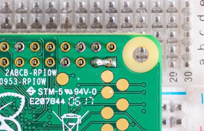
A solder bridge formed between pins.
As illustrated in the image above, through-hole components experience bridging due to the structures of pins and plated holes and the wave solder process often used to assemble them
What can you do to prevent solder bridges?
While there is no way to guarantee you never see solder bridges on your circuit boards, there are a few key things you can do in your design and preparation to greatly reduce your solder bridging risk.
· Use the correct lead lengths for through-hole parts
Through-hole components with leads that are too long can cause solder bridges. The correct lead lengths for your application will depend on the size and thickness of your PCB, the size and mass of the component, and the type of soldering you plan to employ (wave, selective, etc).
It is worth investigating this ahead of time to reduce your rework time after the fact. A good printed circuit board assembly house will be able to help you.
· Use the correct hole size and pad diameter for through-hole parts
Many solder bridges are the result of holes and/or surface pads that are too large. An annular ring pad that is too large decreases the distance between the solderable surfaces of two adjacent pins. This decreased distance, especially in a wave solder operation, greatly increases the risk of a solder bridge. So follow datasheets to correctly size both the plated through hole and the pad.
· Design to the highest producibility level possible
Designing for producibility applies to both surface-mount and through-hole components and relates to the ease of producibility given the dimensions and spacings of your land patterns for your parts.
The IPC (Association Connecting Electronics Industries) publishes industry standards for PCB design and assembly, and they have defined Level A as the preferred level for general producibility. In some designs very small spacings are unavoidable, but in many designs, they are very avoidable. The best practice here is to avoid using unnecessarily small parts or tight spacings.

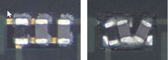
01005 parts
· Properly apply solder masking
Solder mask is the coating on the top of the PCB that is applied everywhere that solder is not desired. Solder inherently does not want to adhere to solder mask, which is a kind of epoxy in most cases. Solder mask should be applied everywhere, especially between the pins of your components. Not applying solder mask between the pins, whether on purpose or inadvertently, creates a high solder bridging risk.
· Place fiducials on your PCB
Fiducial marks are precisely designed markers that you put into your PCB design to allow an automated machine to find your PCB and align placement of every part on your board. When used correctly, component placement and alignment is easy.
The IPC recommends three fiducial marks, two in opposite corners and one in another corner. Most PCB assembly houses will accept just the two in opposite corners. Using poor fiducial marks or poorly placed marks will increase the risk of misplaced parts, which in turn increases the risk of solder bridges.
Capabilities
Payment Methods
Specials Price
Carriers
Support Hobbyist
Certificate
Customer Support
Follow Us
Tel: 1-905-339-2881
Email: sales@goldphoenixpcb.com , tech@goldphoenixpcb.com
Copyright Gold Phoenix PCB Co., Ltd. 2011 - 2026
Tel: 1-905-339-2881 Email: sales@goldphoenixpcb.com , tech@goldphoenixpcb.com
Quality Control System
|
Products/Service
|
Friendly Links
Copyright Gold Phoenix PCB Co., Ltd. 2011 - 2026


