Surface Mount Assembly Procedure of PoP Components
Package on package (PoP) is an integrated circuit packaging method to combine vertically discrete logic and memory ball grid array (BGA) packages. Two or more packages are installed atop each other, i.e. stacked, with a standard interface to route signals between them.
The PoP technology occurs to cater to electronics industry's constantly demands of fine pitch, smaller size, high signal processing speed and smaller mounting real estate towards electronic products such as smart phones and digital cameras. When applying this technology in the PCB assembly process, electric connection occurs between memory devices at upper package and logic devices at lower package, those devices can even be tested and replaced alone. All of these features help reduce PCB assembly costs and complexity.
PoP Structure
There're two widely used PoP structure, namely Standard PoP Structure and TMV PoP Structure.
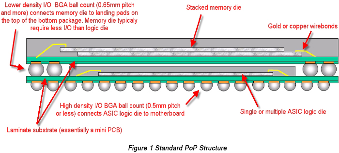
Standard PoP Structure
In a standard PoP, logic devices are placed at the bottom package and logic devices feature a structure of fine pitch BGA solder in harmony with device's attribute of a large number of pin counts. The top package in the structure of a standard PoP contains memory devices or stacked memories. Owing to insufficient pin counts memory devices contain, margin array can be applied so that interconnections between memory devices and logic devices at the margin of two packages.
Currently wire bonds are fast being replaced by flip chip technology in bottom package to meet higher demands of smaller package size, which cause solder pitch in bottom package constantly going down. 0.4mm solder pitch has been commonly applied in bottom package. Moreover, both dynamic random-access memory (DRAM) chip and DRAM chip containing flash memory in upper package strive for higher speed and bandwidth. Correspondingly, top package should have more solders, which make it necessary to reduce solder pitch of upper package. Initially, a pitch of 0.65mm was far sufficient while finer pitch is currently required. Just like what was mentioned just now, a pitch of 0.4mm has been widely applied in PoP structure.

Miniaturization through high integration is the key element contributing to wide popularity of PoP. Leading elements determining PoP size include:
Maximum size of a bare logic device;
I/O interface counts for logic devices;
Overall bus count of power and ground;
Dimensions of memory devices in upper package that provide overall I/O, power, ground and mechanical support;
High-density wiring and cross network required by configuration of logic and memory devices integrated in BGA;
The overall solder count demanded by bottom package and concerning area.
TMV PoP Structure
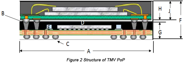
Through mold vias (TMV) PoP, a creation and improvement based on standard PoP, has been widely applied in handheld electronic applications owing to its merit of fine pitch. Figure 2 displays the structure of TMV PoP.

The following table indicates the leading dimensions of a structure of TMV PoP.
Package (A) | Upper solder | Bottom solder | Silicon wafer (D) | Passive | Stacked package (F) | |
14*14mm | Pitch: 0.5mm | Pitch: 0.4mm | 7.10mm*6.97mm*0.13mm | Size: 0105 | Through mold top: 0.40 | |
In a TMV PoP, through mold vias are responsible for electric connection between logic device in top package and memory device in bottom package which is achieved by through mold vias in bottom package and between top solder in bottom package and solder in top package. Both solders in top package and bottom package were spherical solder prior to soldering after which they became cylindrical objects B points to like those in Figure 2.
TMV PoP is expected to be capable of shrinking package size, thickness and warpage. Moreover, it allows the next generation of PoP to achieve higher interconnection density, performance and reliability. Its advantages include:
Broke bottleneck between pitch and package clearance, help meet demands of increasing memory interface density.
Balanced fully-molded structure is beneficial to warpage control so as to meet the demand of reducing bottom package thickness.
Dimension ratio is added between chip and package.
Contributive to configuration of wire bonding, FC, stacked chip and passive component.
Help increase reliability of top components and bottom through mold vias are capable of holding solders with larger volume, supporting larger stand-off height and improving stress distribution of thermal cycling.
SMT Assembly Techniques of PoP
When it comes to surface mount technology (SMT) modes of PoP, two types of technologies are available: pre-stacked PoP and on-board stacking PoP.
In pre-stacked PoP technique, manufacturers will stack top package and bottom package, carry out soldering to make the combination be a component that is called pre-stacked device, then attach the combined component to printed circuit board (PCB) surface and implement reflow soldering.
In on-board stacking PoP technique, manufacturers will sequently stack bottom package and top package on circuit board. First, they will mount bottom package on circuit board, then mount top package on bottom package after dipping into flux or solder paste. Next, conduct a reflow soldering on the stacking package.
Take a double-side SMT assembly as an example, steps of on-board stacking PoP assembly include:
Non-PoP side component assembly (printing, mounting, reflow soldering and inspection);
Solder paste printing on PoP side;
Bottom package and other devices mounting;
Top package devices dipping flux or solder paste;
Top package mounting;
Reflow soldering;
Inspection (X-ray or AOI).
Compared with pre-stacked PoP SMT assembly technique, on-board stacking PoP contains two more steps: top package's flux or solder paste dipping and top component mounting.
SMT Procedure of PoP Components
Step One: Solder Paste Printing of PoP Bottom Package
Solder paste printing of PoP bottom package is determined by component size, pad size and clearance between components. Wide applications of 01005 and high-density CSP (chip scale package), clearance has developed from 0.1-0.15mm and stencil printing clearance falls in the range from 4-5mil. To meet such increasing requirement, laser-cut and/or ladder stencil template by electroforming is usually applied. Solder paste is selected based on printing clearance. Many companies start to use Type IV solder paste while Type III solder paste is still applied in many situations.
Bottom package of PoP assembly is the same as BGA (ball grid array) and CSP assembly in terms of solder paste printing control technique so no remarkable differentiations have been found between bottom package PoP and other fine-pitch components. Printing quality inspection can be achieved with printer or AOI (Automated Optical Inspection) equipment.
Step Two: PoP Top Package Dipping
Either solder paste dipping or flux dipping, all mounting systems have to consider integrated dipping module so as to successfully achieve top package dipping. During dipping, the overall dipping capacity has to be considered. With the improvement of contact area, stress brought by PoP to the surface of solder paste goes up correspondingly. To avoid insufficient or incomplete solder paste picking, it's recommended to modify absorbing capacity or the area WHERE an absorbing tool works. Prior to surface mounting assembly, any transverse movement between solder paste surface and PoP stacking will definitely contribute to possibility of badly-performed wettability on soldering ends. Solder paste has to be eliminated that is peripheral to soldering ends prior to reflow soldering, or soldering defects might be caused.
It's significant to closely observe the changes of solder paste surface after dipping. Solder paste thickness is controlled by scraping blade that moves hard on the surface of solder paste.
After dipping and before surface mounting, positioning inspection system owned by surface mounting equipment should be able to inspect solder paste or flux draining and insufficiency on solders and to inspect excess solder paste on solders as well. Unsuitable dipping thickness or solder paste viscosity changes possibly lead to changes of dipping solder paste volume. Furthermore, owing to environmental changes, long waiting time in a tray and time of exposure to time possibly drive changes in terms of attributes of solder paste.
Great challenges to solder inspection after dipping and before surface mounting occur due to color recognition issues. Some visual modifications can be seen on solders after flux dipping when it comes to PoP and FC. To meet AOI demands, flux suppliers must color flux. Currently, colorants such as white, black and red are widely applied in flux.
Both solder paste dipping and flux dipping have to rest assured that reliable volume of solder paste or flux can be achieved. When it comes to specific applications, experiment or optimization can be relied but for issues that fail to be evaluated, other methods should be explored. For example, it's relatively a hard job to judge the volume of dipping flux and volume of solder paste dipping should be evaluated through observations of weight modification after dipping.
To obtain excellent dipping effect, a couple of significant elements have to be ensured by solder paste dipping and flux dipping, including: homogeneity, staying time on a tray, consistency between dipping amount and volume, and waiting time prior to reflow soldering after dipping.
Section
Surface Mount Assembly Procedure of PoP Components_1
Surface Mount Assembly Procedure of PoP Components_2
Capabilities
Payment Methods
Specials Price
Carriers
Support Hobbyist
Certificate
Customer Support
Follow Us
Tel: 1-905-339-2881
Email: sales@goldphoenixpcb.com , tech@goldphoenixpcb.com
Copyright Gold Phoenix PCB Co., Ltd. 2011 - 2026
Tel: 1-905-339-2881 Email: sales@goldphoenixpcb.com , tech@goldphoenixpcb.com
Quality Control System
|
Products/Service
|
Friendly Links
Copyright Gold Phoenix PCB Co., Ltd. 2011 - 2026


